PIN IN PASTE APPLICATION
INTRODUCTION
The Pin in Paste method, also called through-hole reflow technology, has become increasingly important during the past few years. Reaching a higher degree of automation with existing manufacturing equipment is one primary advantage. Further advantages are as follows:
• Elimination of the soldering by hand or wave methods
• Reduction in manufacturing floor space
• Reduction in manufacturing equipment - consequently in investment cost
• Compatible with the existing processes
• Use of no-clean soldering process possible
• Higher reliability at PC board level due to fewer soldering processes
• Lower heating stress at the component level
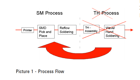
Through Hole Reflow Technology provides a method to switch TH components to the SM process without losing the advantage that TH components offer. Additionally, extensive changes at the board and process levels may not be necessary. If OEM’s and contract manufacturers would like to consider Through Hole Reflow Technology, they must consider that the specification of the SM assembly process has to be compatible with the specifications of the TH components. The main requirement of the TH components is to withstand the direct exposure to high temperatures during reflow soldering. Additional requirements to be considered is component handling by automatic pick & place equipment and modification of the solder paste printing process. With the correct modifications of the assembly process, the manufacturer can ensure the quality and long term reliability of the solder joint.
TECHNOLOGY
The current production process of electronic boards consists of two main steps component placement and soldering. During Step 1, the PC board will be populated with surface mount components (SM) and soldered by reflow. During Step 2, through-hole components (TH) are mounted and soldered by hand or wave. To eliminate Step 2, all TH components would have to be switched to equivalent SM parts. The problem occurs that some equivalent SM parts are simply not available on the market or due to electrical and mechanical limitations, a solution is not possible.
REQUIREMENTS ON THE COMPONENT
Temperature
During wave soldering, the heat attacks the TH component via direct conduction through the wire leads. With reflow soldering, the entire component (casing + terminals) must withstand temperatures up to 260°C over several seconds.
Packaging
The components are available in standard packaging for use in pick & place equipment. Fuses are delivered on tape with a width of 16mm. Due to the special structure of the tape; the leads are always positioned in the same direction to facilitate the mounting process. This makes the handling easier and saves assembly time.
Stand-Off Housing
The construction of the component‘s housing should allow a visual inspection of the solder joint. Additionally, a stand-off pad underneath the component’s body is very important to ensure that there is no contact with the solder paste during reflows. The planar surface on top of the component makes it easy for vacuum pick up in the center with pick & place equipment.
DESIGN REQUIRMEMENTS
Hole Diameter
Trials and tests with the sample board have shown a hole diameter of 0.9 –1.1 mm is an optimum value for fuses WHERE the pin diameter is 0.6mm. The hole diameter is measured at the end of the PC board manufacturing process including the plating. If the PCB hole diameter is too small, it is very difficult to fill the hole properly with paste during solder paste printing. Low solder volume can cause a low quality solder connection. On the other hand, an oversized hole requires too much solder. In this case, multiple printing steps may be required to properly fill oversized holes.
Lead Length
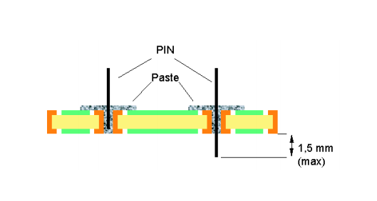
The required lead length of the component is dependent on the thickness of the PC board. Of particular importance is whether the leads can jut out through the hole on the bottom of the PC board or not. If not, only one solder fillet is on the top side and did not affect the components on the bottom side. Very long leads can push out too much paste and thus during reflow soldering, the solder cannot flow back to the solder joint. Please note that if the lead length is longer than the board thickness, the lead length protruding from the bottom of the board should not exceed 1.5mm. The thickness of our sample board is 1.55mm, whereby the component lead length is 1.4 mm.
PROCESS REQUIRMENTS
Solder Volume
Sometimes overprinting and printing on the board’s solder mask is necessary to reach the required solder paste volume. Due to this fact, the solder paste should be compatible with the solder mask material used on the board. The ideal combination leaves no excess solder residue behind during reflow. All solder should flow back to the solder joint. Our recommendation is to test the compatibility between solder paste and solder mask material before implementing Through-Hole Reflow Technology.
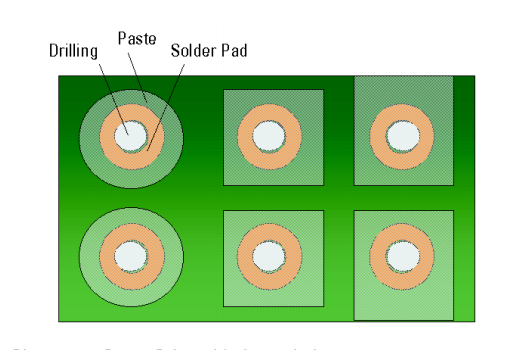
The solder paste volume is calculated as follows.
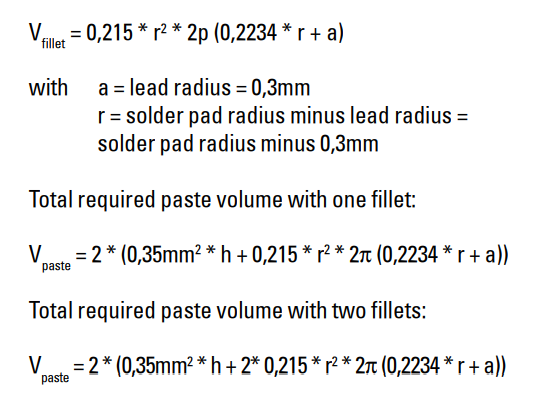
Solder paste contains about 50% of metal material. The other part is additional material which oozes out during the reflow process. Therefore the required paste volume is double that of the calculated total volume.

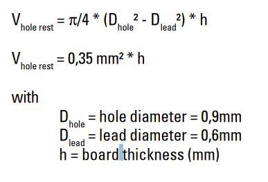
The total volume of the paste required is calculated by the hole volume (Vhole) minus the lead volume (Vlead). In case the lead does not jut out of the hole on the bottom of the board, the fillet has to be added once. Otherwise, the fillet needs to be added twice.
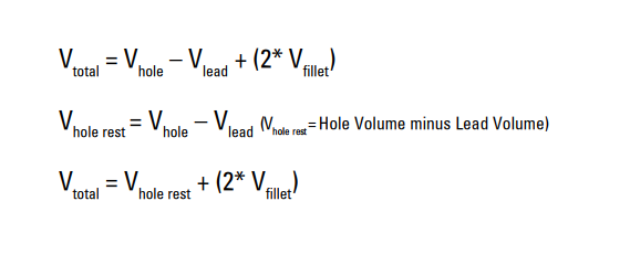
Hole Volume Calculation
Fillet Volume Calculation

Solder Paste Printing
In order to dispense the solder paste on the board, different methods are possible. Some companies use solders paste dispensers where the paste is pressed through special nozzles. Printing using a stencil is the most common method. The thickness of the stencil is dependent on the lowest pitch component on the board - in a range of 75μm – 300μm. With a variation of the aperture size, the required paste volume can be properly controlled. In general, the aperture size must cover the hole and solder pad.
Printing
Best results are obtained when printing twice onto a board without separating the PCB and stencil. During the second printing step no additional paste is applied onto the surface mount pads, but paste will flow deeper into the through-hole drillings. Another method involves printing the paste twice, but using a second separate stencil. During the first step, the paste for TH components is forced into the hole. Then, with the second stencil in place, additional paste will be added to the hole as well as to the TH solder pads and SM parts. Two stencils and printers are required for this method. A further solution is to use a stepped stencil. The paste for SM components will be printed first. During the second printing step, paste is applied into the hole using a second stencil with etched recesses on the bottom side. The etched recesses are needed to prevent the first print from blurring.
Paste
It is not easy to offer a recommendation with regard to the solder paste as there are so many different types on the market. The following requirements are basic characteristics. High viscosity is required during time of application. If the paste dries too fast after printing, it is possible that the lead will press too much paste through the hole. With a low viscosity, the paste is unstable and may not properly cover the hole. The paste must be applied with the correct viscosity and robustness for the solder process to be successful.
Quality
The pilot test batches have been inspected visually according to IPC 610B class B. The tests are based on the acceptance criteria for electrical components for soldering joints of through-hole components. Non-visible areas were checked by means of polished cross-cut images. The following criteria served as a basis:
• A minimum of 75% solder coverage on both sides of the wire leads
• Less than 30% air cavities
• 100% wetting at the surface of the drilling hole and on the component lead.
The soldering results showed no deviations from the IPC Standard. The results showed a good solder connection without an increase of cavitation shrink holes.
Capabilities
Payment Methods
Specials Price
Carriers
Support Hobbyist
Certificate
Customer Support
Follow Us
Tel: 1-905-339-2881
Email: [email protected] , [email protected]
Copyright Gold Phoenix PCB Co., Ltd. 2011 - 2023
Tel: 1-905-339-2881 Email: [email protected] , [email protected]
Quality Control System
|
Products/Service
|
Friendly Links
Copyright Gold Phoenix PCB Co., Ltd. 2011 - 2023


