PCB PLUG VIA PROCESS
Primary LPI Solder Mask Tenting Vias
In tenting vias, no apertures are supplied on the mask data layer. The solder mask covers the via pads and tents hole. No surface finish is applied to the via barrel. For this process it is possible for entrapment to occur.
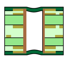
In the past, tenting of vias with Dry Film Soldermask was a standard offering. Due to the limitations on feature size resolution and high thickness for SMT applications of the Dry Film Masks, this process is not readily available. Assemblers may require plugged vias due to vacuum draw or to prevent paste wicking into vias.
This process is not advised for long term reliability. Many printed circuit board designs are seen with vias tented via primary mask. This could be a result of a lack of reliability data.
Pros:
The pros to primary LPI solder mask tenting vias is it is only a one step application.
Cons:
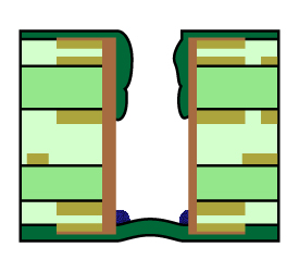
Via tenting cannot be guaranteed with LPI mask. There are three common methods of applying LPI mask. Curtain, Spray and Screen coating. Curtain and Spray coating cannot ensure that the via is tented both sides. Screen coating’s ability to tent is limited by the hole size, surface tension of the liquid mask, and board thickness.
If a via is not tented on both sides, chemical entrapment from surface finish preclean lines is probable. All the finishes will be subject to a micro-etch process. The micro-etchant that gets trapped in the capped via will crystallize rapidly causing copper sulfate crystals. Over time, these crystals can cause long term reliability issues. In the case on ENIG finish, the gold and small area of exposed copper near the cap could form a galvanic cell, accelerating the etch process.
Vias Not Covered
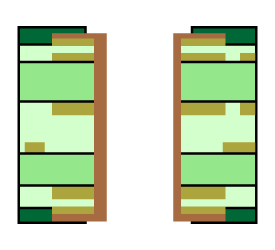
If vias are not covered, they are exposed and the surface finish is applied to via barrel. This is standard process in printed circuit board fabrication.
Pros:
The via barrels are covered with surface finish metal. This allows circuit board testing access available from both sides of the board.
Cons:
It is possible for wicking of solder paste to get into the via. In the case of BGA rework, paste loss due to wicking into the via is a result of the localized thermal energy causing the LPI solder mask to lift on the short distance between the ball and via capture pads. This is not a concern at first pass assembly.
Button Print
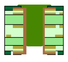
In the process, vias are tented on one side by a secondary solder mask application. The surface finish is applied to the via barrel prior to button print.
This process was developed to allow a rework able, reliable via interconnect.
Pros:
The via barrels are covered with the surface finish metal. Test access is only available from one side of the board. This is rework able as solder wicking is not a concern. Button print vias are a standard industry process in fabricating printed circuit boards.
Cons:
This can cause perceived mask height issues at the time of assembly. The industry maximum height of soldermask over copper has been reduced over the years from 0.004" down to 0.002". This may require an additional mask application process, post surface finish application. This process is not recommended for OSP or Tin finish and the depth of mask cannot be controlled.
Plugged Via
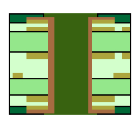
In the plugged vias process, vias are plugged with solder mask or some other non conductive media. LPI mask is then applied over plug. During the plugged vias process, no surface finish is applied to via barrel.
This process was developed as a modification from the LPI tent to guarantee that 100% of the vias are fully tented.
Pros:
In plugged vias, 100% of the required vias are tented.
Cons:
For plugged vias, additional process steps are required during fabrication. No surface finish is applied to the via and the via size is restrictive. The control of rate of rise during curing is critical to ensure 100% of volatiles are evacuated. Failure to control this can lead to soldermask smearing the surface during the assembly reflow process.
Active Pad
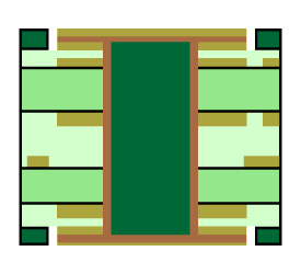
In the active pad process, vias are plugged with a conductive or non-conductive media, then planarized and plated over.
This process allows the use of via capture pads as SMT pads. This is advised for via in pad applications only.
Pros:
For active pad vias, this reduces the routing issues on external circuit layers and minimizes inductance.
Cons:
During the active pad process, additional process steps are required in addition to a dual plating processes. The extra plating processes have a negative effect on the minimum feature size capable on the external circuit layers. This process is not advised in conjunction with PTFE substrates.
Capabilities
Payment Methods
Specials Price
Carriers
Support Hobbyist
Certificate
Customer Support
Follow Us
Tel: 1-905-339-2881
Email: [email protected] , [email protected]
Copyright Gold Phoenix PCB Co., Ltd. 2011 - 2023
Tel: 1-905-339-2881 Email: [email protected] , [email protected]
Quality Control System
|
Products/Service
|
Friendly Links
Copyright Gold Phoenix PCB Co., Ltd. 2011 - 2023


